Pcb Strain Gauge Testing

A Illustration Of Strain Gauge Locations On The Front Side Of Pcb Download Scientific Diagram
Pcb Strain Testing Shama Technologies

Rf9 Printed Circuit Board Testing Hbm

Strain Gages For Measuring Strain And Stress On A Pcb Kyowa Americas Inc
Https Www Keysight Com Upload Cmc Upload All Boardstrainanalysisprocesspdf Pdf

Miniature Planar Rosette Strain Gauge Pattern For Pcb Testing Engineer Live
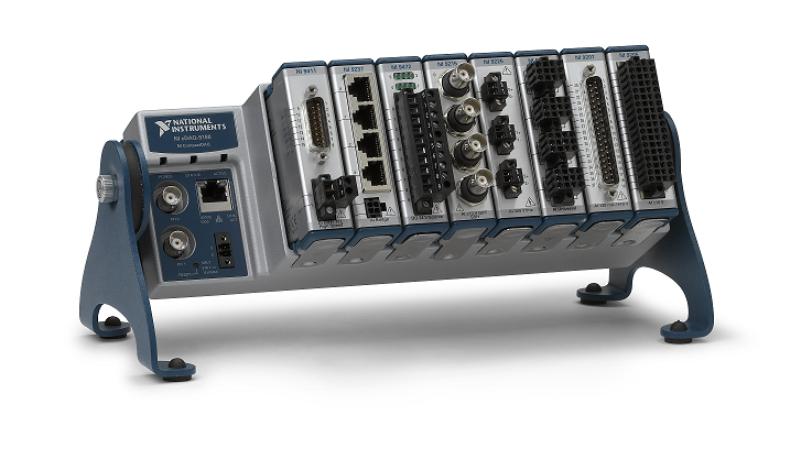
With flexible software and modular hardware ni offers scalable systems that can meet your needs for pcb strain gage testing.
Pcb strain gauge testing. This high resolution dynamic alternative to bond foil strain gauges uses a quartz sensing element in a durable titanium housing. Conventional strain sensors are based on strain gage technology. Pcb strain gage testing addresses one of these challenges by proactively identifying high stress inducing and potentially damaging processes in the manufacture of pcb based products. We have made it our business to make the strain measurement of printed circuit boards according to ipc jedec 9704 as uncomplicated and reliable as possible for this reason we will soon introduce our new pcb testing kit from the strain gauge to the measuring amplifier and the pre configured measuring project.
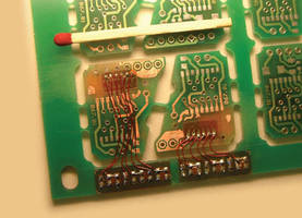
Model 740b02 for dynamic testing of aircraft defense vehicles and components. Strain gage placement for intel bga components plan of record location and alternate gage locations. Using ipc jedec 9704 9702 standards for strain gage testing of any printed wiring boards. The c2a 06 g1350 120 rectangular rosette gauge and c2a 06 015lw 120 uniaxial linear gauge are designed to detect pcb surface strains at critical locations in consumer.
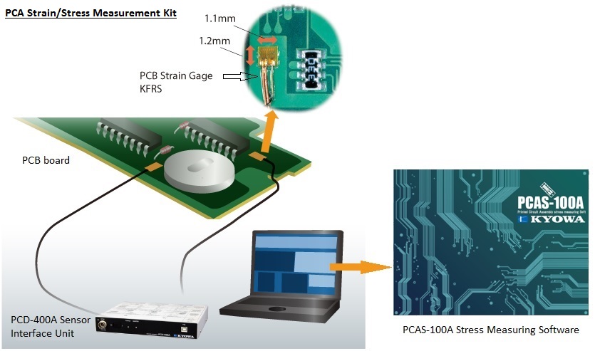
The configuration is known as a wheatstone bridge circuit. Three small scale strain gauges designed to meet the growing demand for precise stable and reliable stress analysis of pcbs even in harsh environments have been introduced by micro measurements a vishay precision group. Pcb strain testing kyowa tm offers a complete printed circuit assembly pca strain stress measurement kit which is suitable for measuring strain stress of printed circuit board pcb thereby providing efficient quality control or quality assurance for pcb boards. The pcb testing kit contains all necessary materials.
In this inotes video mike talks about cracks in the pcbs and shows how micro measurements strain gage sensors are used when testing components sub assemblies printed circuit boards ball grid array bga surface mount packaging and finished products. Since strain is relative to location the same strain gage location must be used for testing as was used to get the strain guidance. A wheatstone bridge has a very linear output in it s midrange. Unless the gages are placed in the same location strain numbers cannot be compared to the strain guidance.

Hoffmann Krippner Announces Polymer Strain Gage Printed Onto A Pcb No More Wires Embedded Computing Design

Strain Gage Attached Close To The Package Corner On The Secondary Side Download Scientific Diagram
Strain Gauges Optimize Pcb Production Quality

Pcb Testing Hbm
Identify And Characterize Damaging Pcb Assembly And Test Processes Using Strain Gage Testing National Instruments

Pcb Testing Services Printed Circuit Boards Hbm

Pcb Bending Test Youtube

Zemic Web English Version

Strain Gauge Stress Testing On Printed Circuits Boardss Youtube
Https Www Mdpi Com 2504 3900 2 8 472 Pdf
Https Www Jor Se Wp Pdf Kyowa Pcas S Pdf

Example Of An Ict Test Environment With Probes And Pushers On The Pcb S Download Scientific Diagram
