Pcb Stackup Design Tool
Pcb Stackup Calculator And Si8000m Controlled Impedance Field Solver Professional Pcb Stack Up Design And Documentation
Pcb Layer Stackup Tool Controlled Impedance Pcb Stack Up Planning Design And Documentation

Top 4 Tips For Pcb Stackup Design Tempo

Pcb Stackup Design Software
Insertion Loss Field Solver Controlled Impedance Pcb Stackup Design And Documentation Tool

Tips For Pcb Stackup Design Youtube
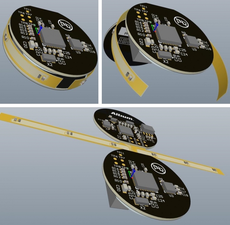
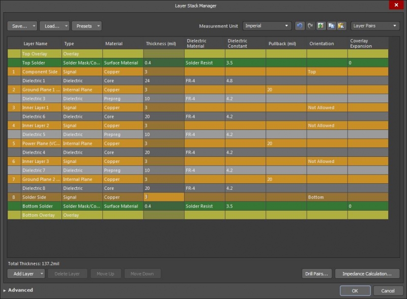
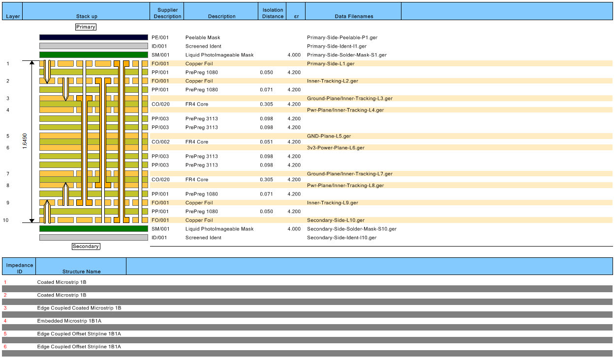
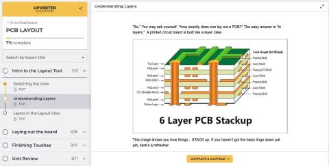
Pcb stackup design example.
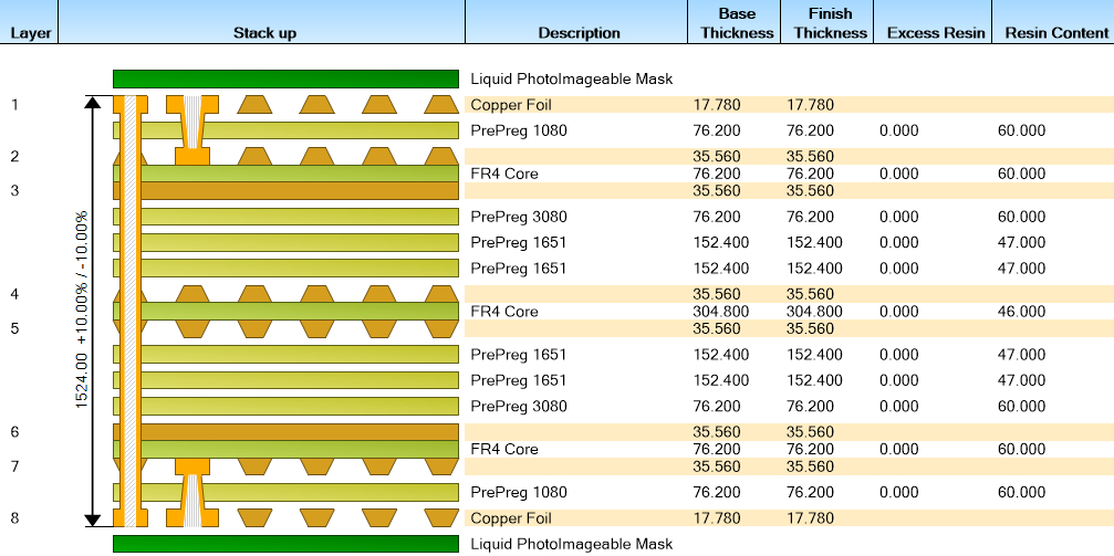
Pcb stackup design tool. However the following illustration is a good reference example for an 8 layer pcb stackup. Digital signature certificate to the program for security. When multiple layers are involved your board design requires you to incorporate a pcb stackup. Polar s industry standard speedstack pcb stackup design tool offers a powerful solution for pcb fabricators and designers when planning and creating live stacks complete with controlled impedance information and professional high quality documentation.
Altium is a pcb design tool that experts recommend for pcb stackup design. Since it was developed at the end of the 20 th century hdi technology which stands for high density interconnection is. Speedstack pcb stackup planning design and documentation. Example 10 layer pcb stackup.
Two four and six layer boards were the usual stackups and occasionally you would see an eight layer design come your way too. Click on the free trial to try it for yourself or watch the ontrack podcast episode with guest lee ritchey below. We will present and explain how our hdi stackup planner our hdi material selector and our impedance calculator work so you can choose which one best suits your needs. In this article you will learn about sierra s 3 free hdi tools essential for hdi pcb design.
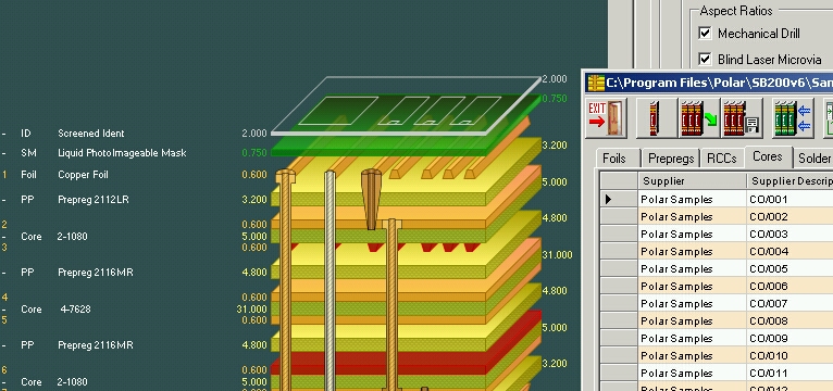
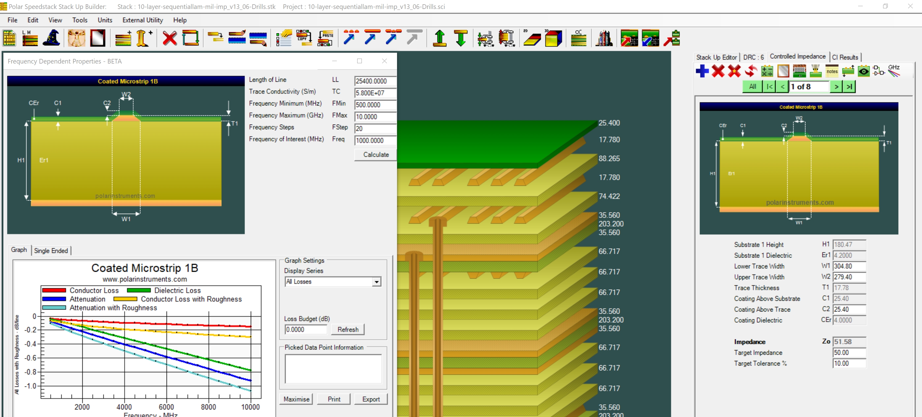
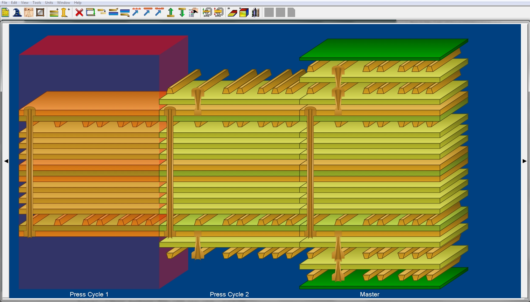
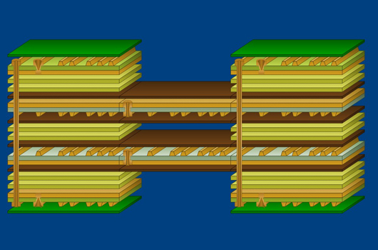
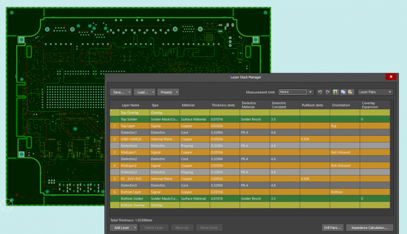
Many possible pcb stackups may be realized depending on your implementation of the above tips. Speedstack stackup editor exploded view of stackup. Fix an issue for comma user where 10 5 was an invalid default value. Changed gbaud s to gbaud in the differential vias tool.
An accurate and detailed pcb stack up at the beginning stages of a layout reduces unnecessary iterations and helps optimize the costs by increasing manufacturability and electrical performance for a given design. Gauss 2d is our 2d field solver for pcb electromagnetic behavior and gauss stack is our stackup design tool featuring design for reliability checks and dimensional stability warpage simulation. Fortunately altium designer has the advanced tools that you want to create the layer stackup that you need. Armed with the knowledge of what you will need in your pcb stack up the next step is to build it in your pcb design tools.
Sign up and try altium 19 today. Added a saturn pcb design inc. Increased maximum conductor length in the conductor properties tab to 1 200 000mils. Speedstack is a comprehensive pcb stackup design environment for pre layout engineers pcb fabricators and value add pcb brokers.
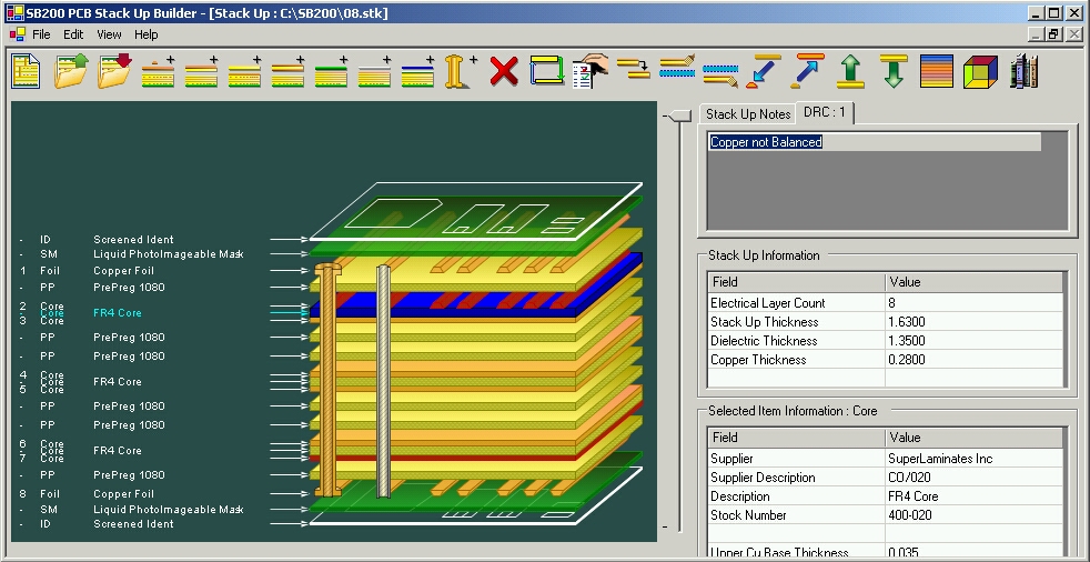
Pcb layer stackup management techniques using your design tools there was a time where most of the circuit boards being designed used the same basic layer stackup. This getting started tutorial will familiarize you with the features and operation of polar s speedstack pcb stackup builder and guide you through the steps to create a speedstack project sci file.

Edn Design Pcbs For Emi Part 2 Basic Stack Up
The Right Software Tools Will Help With Your Layer Stackup In Pcb Design
Pcb Signal Integrity Stackup And Controlled Impedance
Pcb Transmission Line Design And Layer Stackup Tool Package
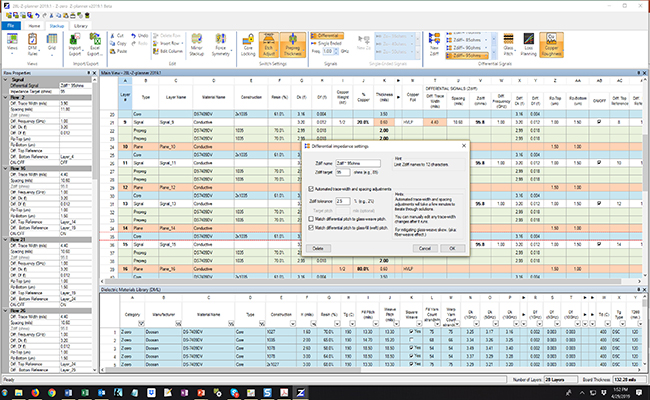
Z Zero Launches V2019 1 Of Z Planner And Z Solver For Pcb Stackup Design 2019 05 06 Signal Integrity Journal
Pcb Stack Up Design Controlled Impedance Calculators Pcb Field Solvers And Test Systems For Controlled Impedance And Pcb Insertion Loss

Polar Speedstack Pcb Stackup Interface Zuken Us
Design Polar Instruments Asia Pacific Pte Ltd
Impedance Calculations And Pcb Stackup Design Altium Com
Z Zero Launches Z Planner And Field Solver Sandbox For Pcb Stackup Design 2017 11 01 Signal Integrity Journal
Altium Empowering The New Generation Of Electronics Designers Afp Com

Pcb Signal Integrity Stackup And Controlled Impedance
Specifying Rigid Pcb Materials In The Stackup