Pcb Stackup Design Considerations

Top 4 Tips For Pcb Stackup Design Tempo
How To Makes A Good Pcb Stack Up News Blog Headpcb Professional Pcb Service Provider

Edn Design Pcbs For Emi Part 2 Basic Stack Up
Everything You Need For Successful Pcb Stackup Design Altium
12 Rules To Properly Design Your Pcb Stackup
Pcb Design Vocabulary Circuit Board Nextpcb
Dfm considerations for ensuring a balanced board pcb guided.
Pcb stackup design considerations. Home blog pcb analysis considerations for every designer. The pcb stackup design perspective that includes both vertical and horizontal considerations is a three dimensional approach that significantly impacts board fabrication and pcb assembly. However lower loss comes at an increased cost tradeoff. 1 pcb stackup design considerations for intel fpgas this application note presents an overview of the pcb stackup construction and material selection criteria.
A pcb layer stack can help you minimize your circuit s vulnerability to external noise as well as minimize radiation and reduce impedance and crosstalk concerns on high speed pcb layouts. Business business international computers and office automation epoxy resins analysis laminated materials laminates physical therapy equipment. The design tools in allegro pcb designer from cadence integrate with a full suite of analysis tools for examining all aspects of signal and power integrity. Pcb stackup design considerations for altera fpgas october 2010 altera corporation ideally selecting the lowest loss material is the best choice.
Insights by printed circuit design fab circuits assembly. For fabrication the number of layers their arrangement or stackup and type of material must be determined. These factors diminish pcb performance margins and require different types of analysis to avoid failures throughout the pcb design cycle. Proper board layer stackup in high speed board design requires the best pcb software and altium designer is a good one to get started with.
The sound pcb stackup strategy part 2. A better approach is to plot equation 1 against. You might want to use the same pcb designer for all your 8 layer pcb stackup needs. That way you are confident that the design will be facilitated in real time and at affordable costs too.
Automotive pcb properties and design considerations electronic elements have been playing an increasingly active role in automotives. There are however some important considerations for the configuration of the stackup that have been listed here that should be helpful to you. Different copper amounts on different sides of a pcb stackup can cause warpage and electrical misfunctions. Besides an 8 layer pcb manufacturer designer that offers a one stop service helps to source the materials and get all the specifications ready for immediate design manufacture and dispatch.
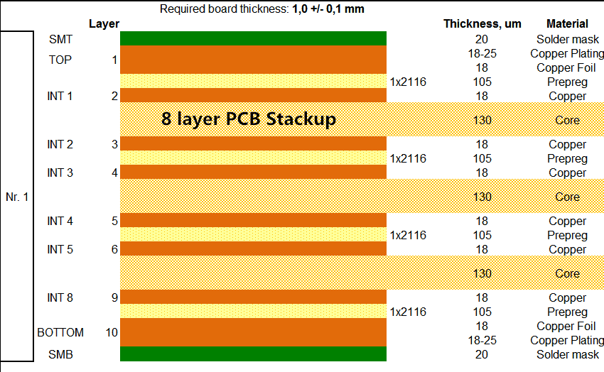
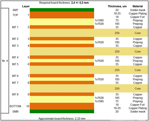
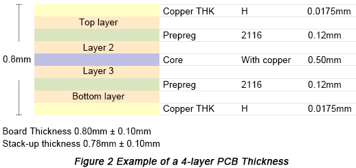
8 Layer Pcb Stackup Meaning Prototype And Guidelines

Pcb Stack Up Planning Elmatica Pcb Broker

Pin By Shawn Wang On Efpcb Products Radio Frequency Innovation Technology Radio
.png)
Multilayer Pcb Manufacturing Process Design Guidelines Pcb Power

Rigid Flexible Pcb Rigid Flex Pcb Ipc Class 3 Pcb Printed Circuit Board Innovation Technology Circuit Board
The Right Software Tools Will Help With Your Layer Stackup In Pcb Design
Pcb Stack Up Plan Design Manufacture Repeat Sierra Circuits
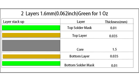
When Should I Choose 2 Layer Pcb Or 4 Layer Pcb
Layer Stackup E3 General Electronics

Pin By Shawn Wang On Efpcb Products Innovation Technology Printed Circuit Board Circuit Board

Repairing A Bad Trace On A Printed Circuit Board Circuit Board Printed Circuit Board Pc Board

Navigating Pcb Stackup Layer Assignments For Optimized Si And Pi Performance In High Speed High Power Designs Semantic Scholar
Pcb Stack Up Design Best Practices With Rick Hartley Ontrack Podcast Altium
