Pcb Fabrication Drawing Example

How To Read A Pcb Fabrication Drawing

Fabrication Drawing Details Layout Kicad Info Forums

Documenting Your Master Drawing Documentation Guidelines Resources Altium
Pcb Soldering Smd Stencil Drawing Example
Pcb Design Guidelines From Qualieco Circuits Australia New Zealand

Altium Pcb Designer Drill Drawing Fab Drawing
When a fabrication drawing is included it is regarded as the blue print of the project and makes clear to the manufacturer exactly what quality and specification requirements are needed to create the desired pcb.
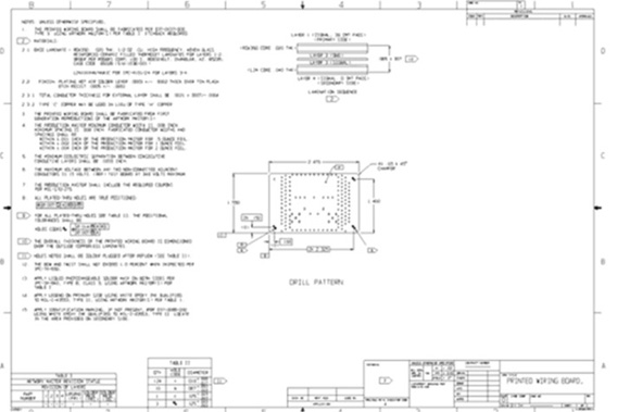
Pcb fabrication drawing example. Pcb pcb fabrication notes primary side shown. Just like crème brûlée is only eggs cream and sugar a fab drawing can be reduced to a handful of basic instructions. Pcb prime sample fabrication drawing. The board illustration shows the actual board outline with all cutouts corners and radii.
Pcb requirements stated clearly from the start. What should be included in a pcb fabrication drawing at bittele electronics we strive to be flexible in our services however there are certain key pieces of information that we must have to accurately fabricate your project. Bow and twist requirements should be noted on the master drawing. Example of pcb fabrication notes.
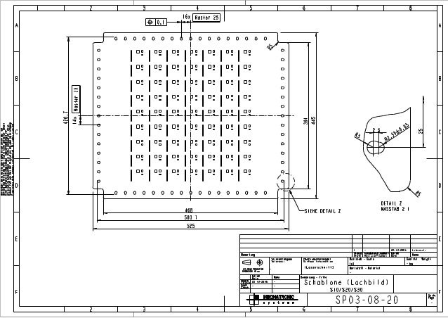
There are four major sections to a fabrication drawing board illustration drill chart section a a notes and title block. Without a fabrication drawing engineers are subject to the default specifications of their manufacturer. Ten layer pcb unless otherwise specified o obo x oo x x xx rev revision description 14 523 14 273 typ. Example of fabrication notes in drawing.
The master drawing is the most crucial part of your pcb documentation. Pcb requirements cost factors 1 manufacturing panel utilization how many pcbs fit on the master panel 2 performance class ipc 6012d class 2 vs 3 3 layer count total number of required cores cores layers 2 2 4 number of lamination cycles each cycle requires lam drill plate etch est 25 per lam cycle 5 design complexity and whether the requirement is standard green. These are some of the most direct and key things to communicate with your drawing. A fabrication drawing specifies how the pcb is to be manufactured.
The clearer this information is made to us the more accurate and faster the quoting and fabrication process will be. Before you find yourself making your printed circuit board purchasing decision based solely on the lowest cost consider what may be omitted from your quote. 13 875 tooling hole ro 060 2x 10 750 10 650 4 825 tooling hole tooling holes 0 300 0 000 size eco no plated yes yes yes yes. Pcb fabrication drawing sample basic ingredients.
From pcb prototype to volume production jlcpcb has guaranteed the delivery of high quality pcbs on time and maintained the customers satisfaction. Most off shore factories go by the gerber as the ruling document but we instruct and push our factories to go by the fab drawing as the ruling document. Jlcpcb is a global leading pcb manufacturer with millions of pcb orders produced per year who provides most efficient economic and innovative pcb solutions for the electronics industry.
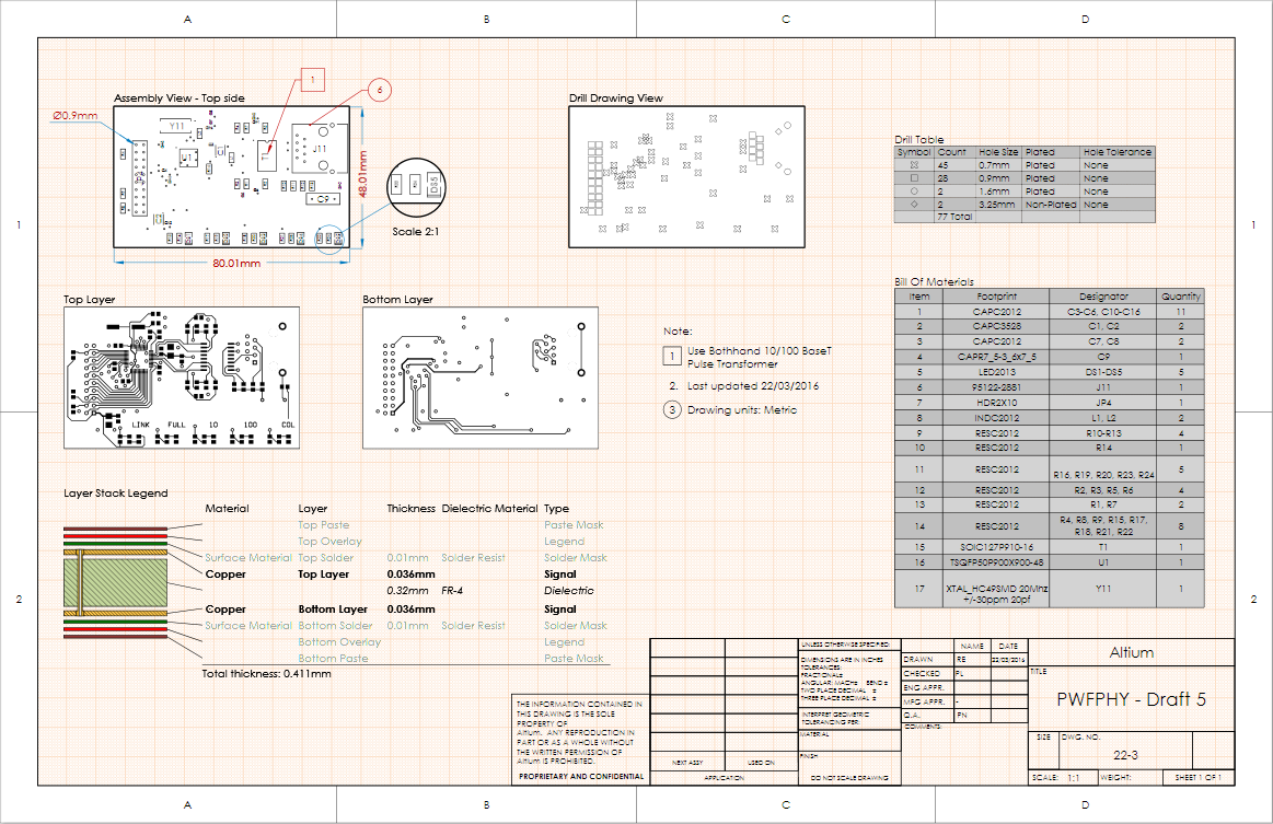
Defining The Layer Stack Altium Designer 20 2 User Manual Documentation
Https Www Ema Eda Com Sites Ema Files Resources Files Allegro Pcb Manufacturing Ds Pdf
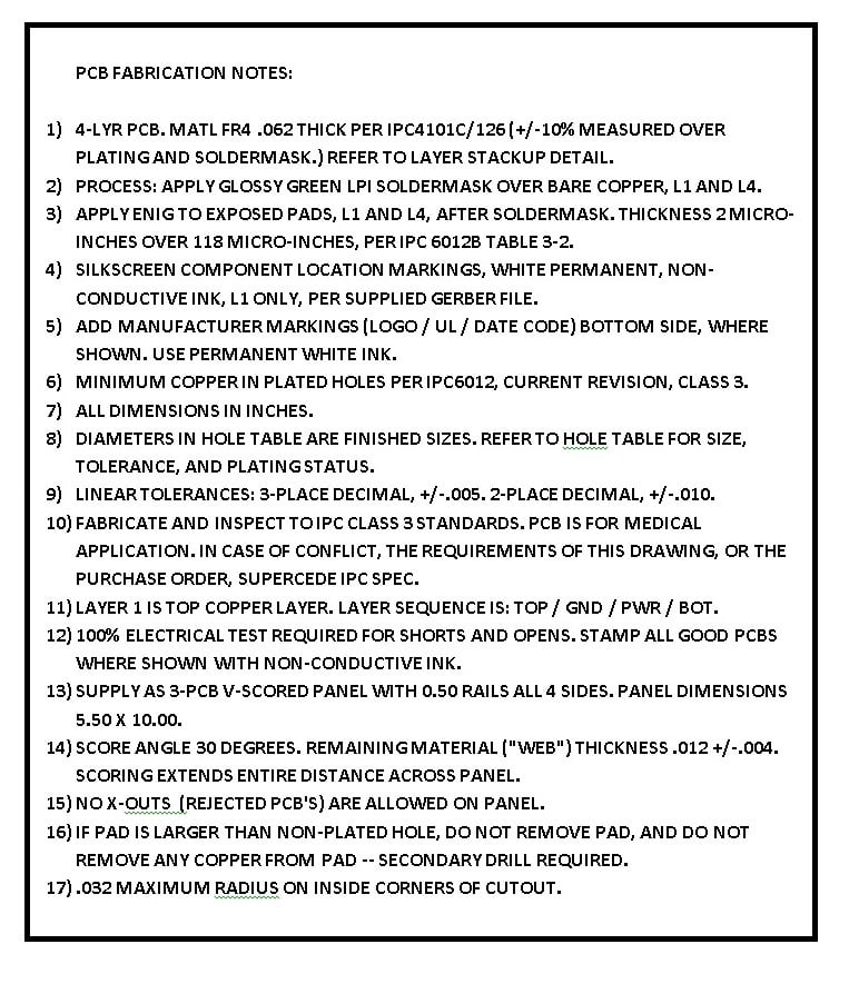
Creating Standard Pcb Fabrication Notes
Recipe For Pcb Design Pcb Fabrication Drawing Blog Altium Designer
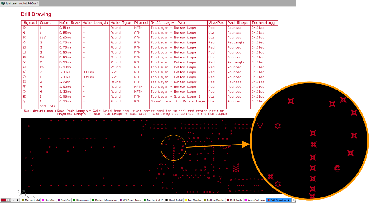
Live Drill Drawing Altium Designer 15 1 User Manual Documentation

Autocad For Pcb Artwork
Pcb Fabrication Data File Requirements
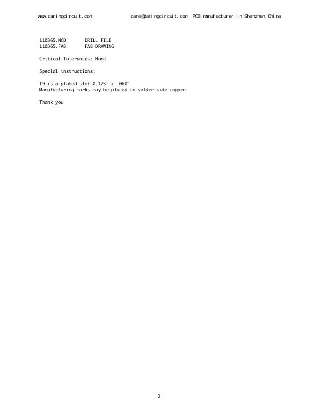
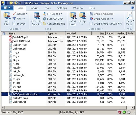
Pcb Gerber Files Readme Sample In Pcb Design Caring Circuit Guideli

14 Things Your Fab House Needs To Know By John Burkhert Jr Supplyframe Medium
Everything You Need For Successful Pcb Stackup Design Altium

How To Do The Pcb Board Array Panelize
Draftsman For Fabrication And Assembly Drawings Documentation Guidelines Resources Altium
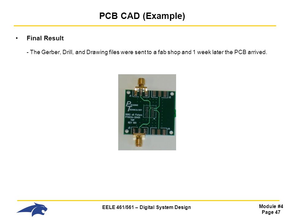
Eele 461 561 Digital System Design Ppt Download
